Flyback Converter
Electronic lab final project
Flyback converter
During my Electrical Engineering Laboratory course, I delved into the world of basic electronic components and their packaging, such as DIP and SMD. Additionally, I learned about layout techniques and how to arrange components to achieve optimal powering stability and reduce noise.
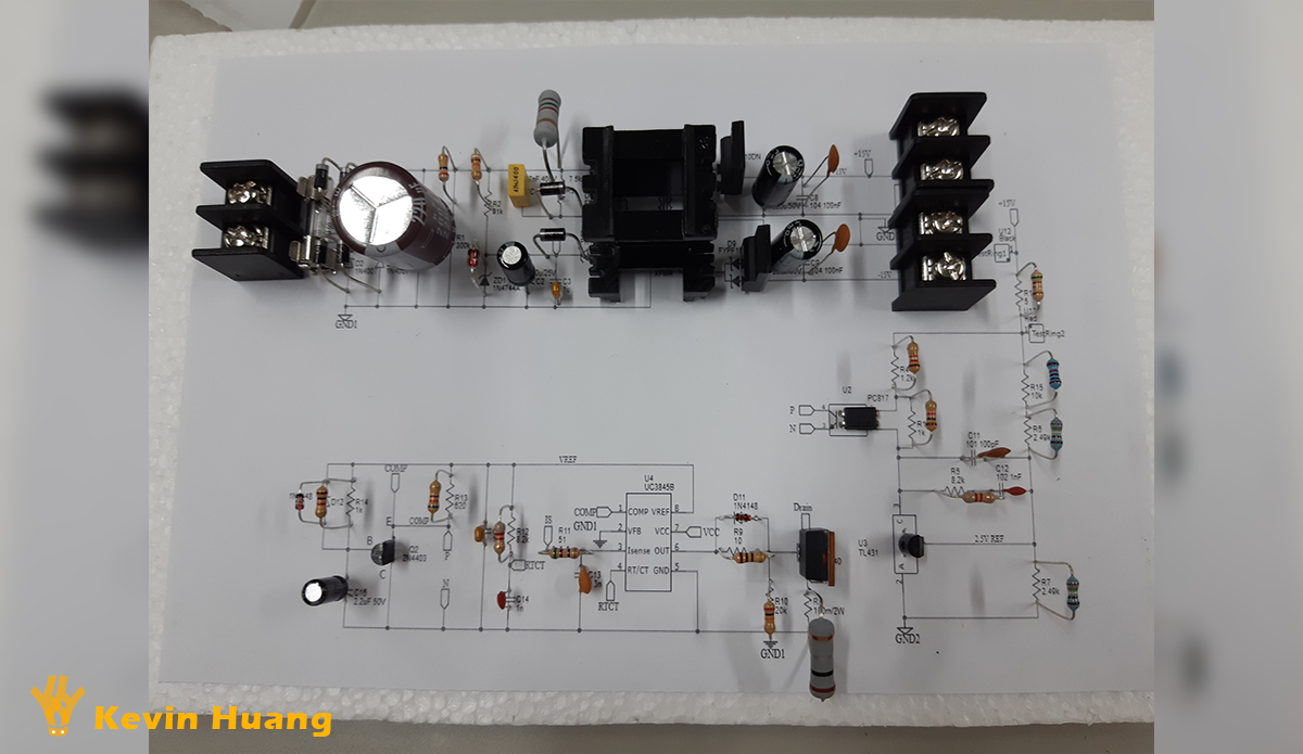 Checking components
| manufacturing PCB | after soldering |
|---|---|
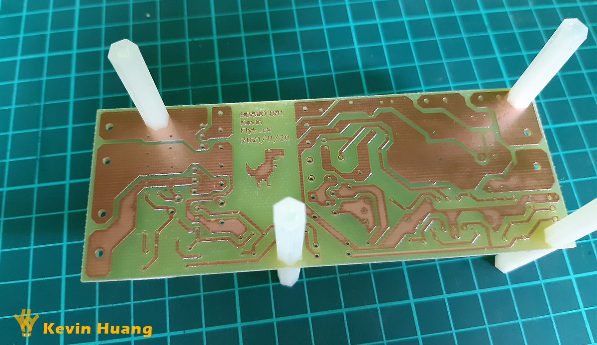 | 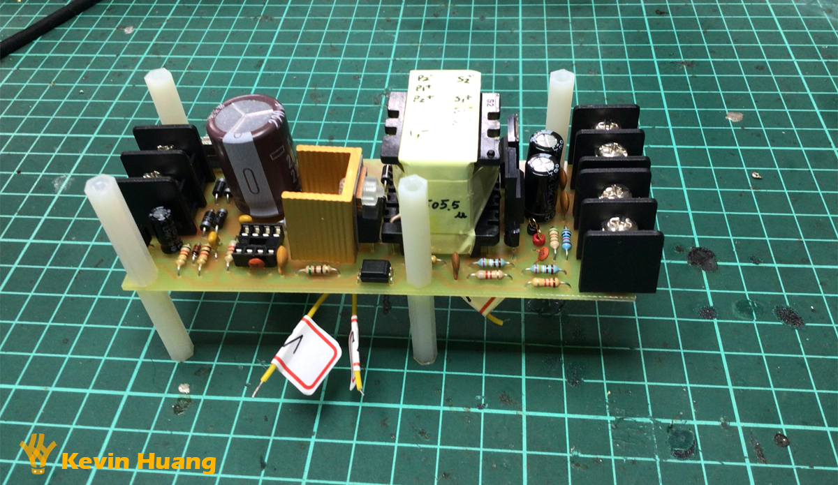 |
For the final project of this lab, we were tasked with designing and implementing a flyback converter capable of converting AC to DC and DC to DC. We began by creating schematics in Spice (Simplis) and simulating voltage and current with some imperfect components. Subsequently, we utilized EasyEDA to draw the schematic, design the layout, and perform Design Rule Checks (DRC). Then we made the board with our CNC machine, and soldered all components onto the board. Finally, we did several testing, including load switching, no load powering, …, and durability testing.
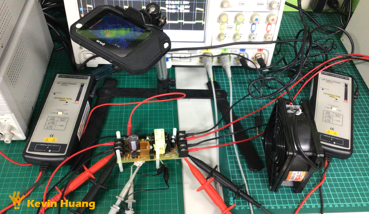 testing setup
This laboratory project proved immensely valuable, as it introduced me to the art of PCB layout, opening the door to designing PCBs for my future projects. I now appreciate the convenience and efficiency of having a well-designed PCB rather than relying on hand-soldering wires and jumpers on a prototyping board. This experience has empowered me with a valuable skillset for implementing professional and reliable electronic circuits in various applications.
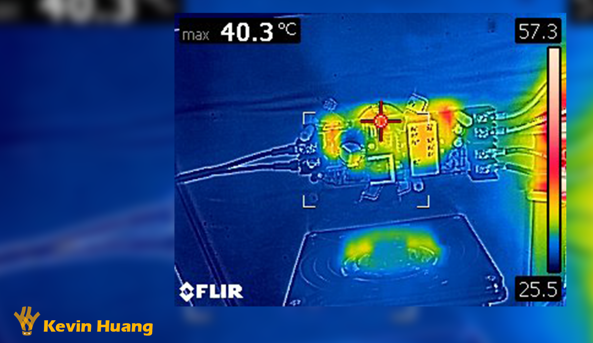 thermal image