
Flyback Converter
A flyback switching power supply designed and built in the EE lab — from schematic simulation to CNC-milled PCB to thermal testing
Flyback Converter
This project was the final assignment for the Electrical Engineering Laboratory course. The goal: design and build a flyback converter — a switching power supply capable of AC-to-DC and DC-to-DC conversion — from scratch, starting with simulation and ending with a working, tested board.
Design Process
The workflow followed a full PCB development cycle:
- Schematic & simulation — drew the circuit in SPICE (Simplis) and simulated voltage/current waveforms with realistic, imperfect component models
- Layout — transferred the schematic to EasyEDA for PCB layout, paying attention to trace routing for power stability and noise reduction, then ran DRC (Design Rule Check)
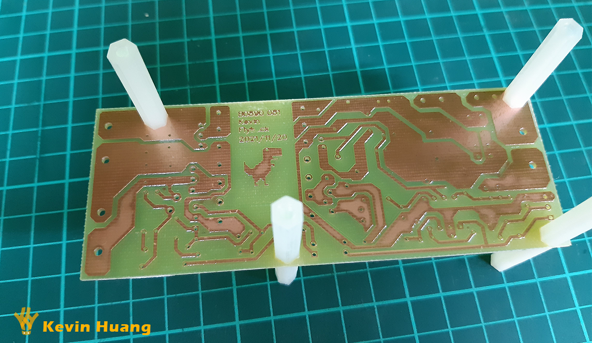
- Fabrication — milled the board on a CNC machine in the lab
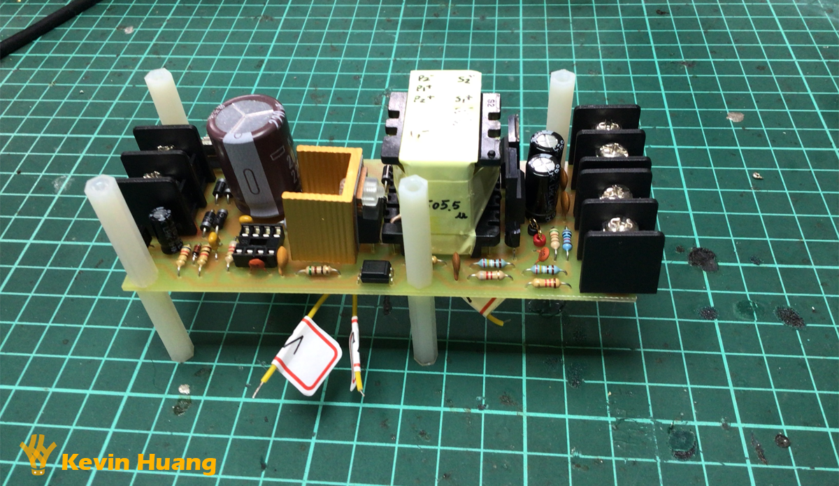
- Assembly — hand-soldered all components, mixing DIP and SMD packages
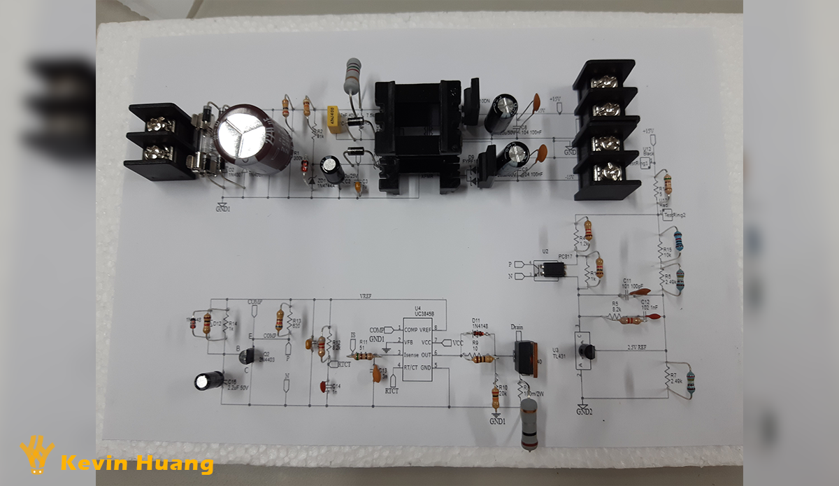
Component placement on the bare board
| CNC-milled PCB | After soldering |
|---|---|
 |
 |
Testing
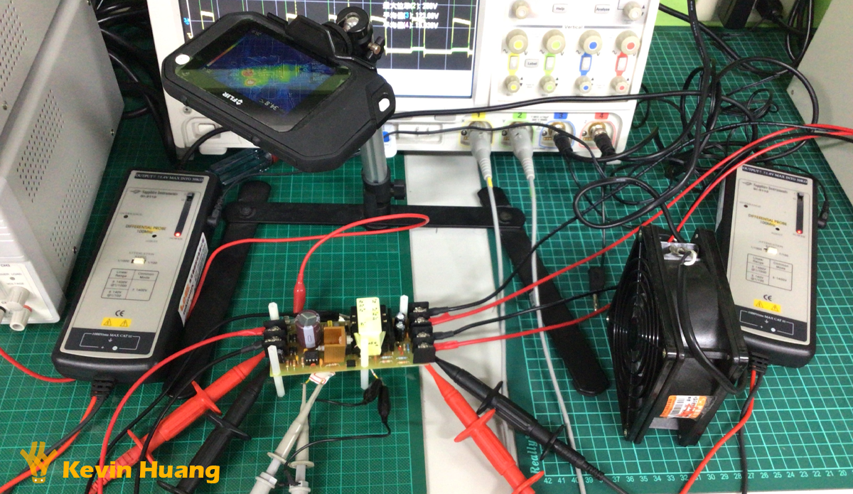
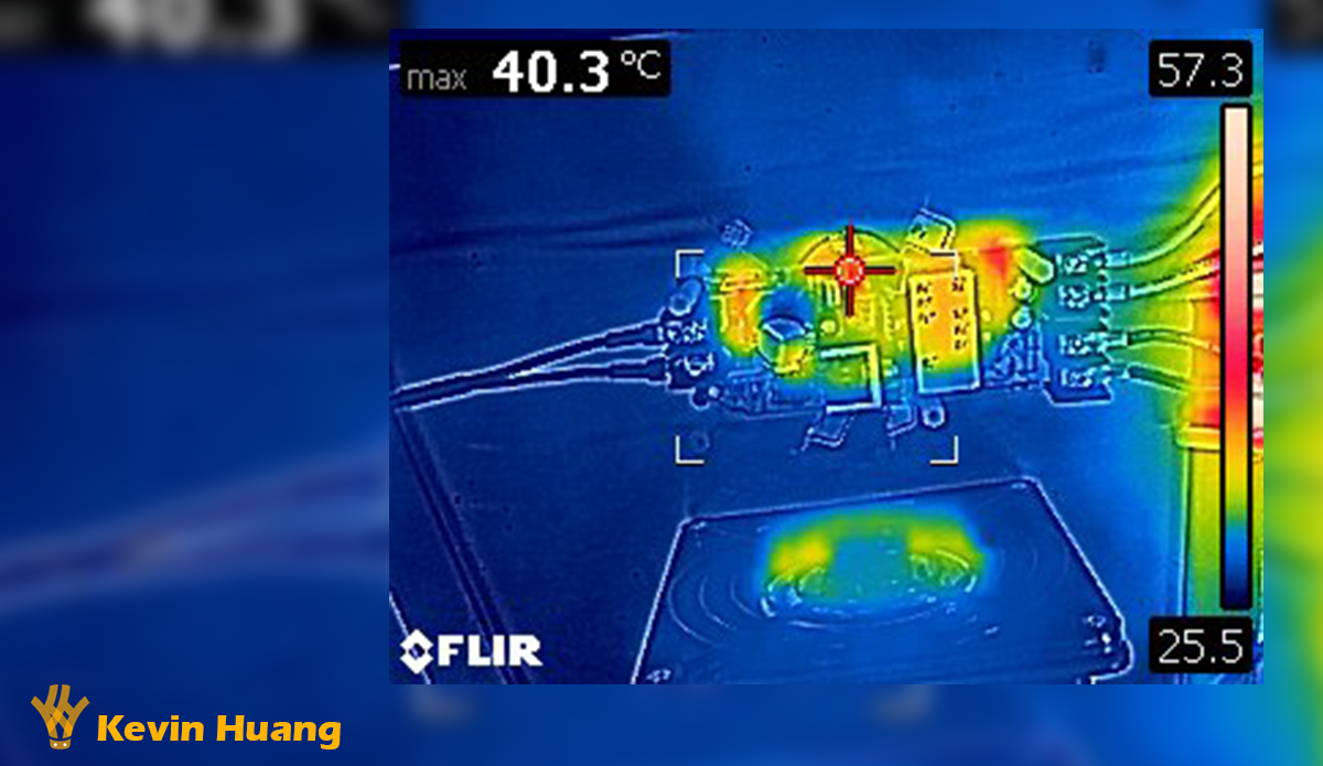
The finished converter went through several rounds of testing: no-load powering, load switching, and durability runs. An oscilloscope verified output voltage ripple and transient response, while a FLIR thermal camera checked for hotspots under sustained load — the board peaked at 40.3°C.
| Test setup | Thermal imaging |
|---|---|
 |
 |